GPLGPU Walkthrough
A few years ago, an interesting kickstarter projected popped up:
https://www.kickstarter.com/projects/725991125/open-source-graphics-processor- gpu
The goal was to publish source code to a GPU that is register compatible with the late 90’s era Number Nine “Ticket To Ride IV” GPU. Although the project didn’t meet its funding goal, the person behind it later published the code on github.
https://github.com/asicguy/gplgpu
Although this is an older design, it has a lots that is worth studying. It’s instructive to compare it to the VideoCore GPU that I walked through in a previous post. While there are some fundamental differences, there are surprising number of similarities, which shows how modern GPUs evolved from earlier ones.
Here are some differences between the two:
- Unlike VideoCore, GPLGPU is a pure fixed function GPU. It does not support shaders or programmable operations.
- GPLGPU does not support vertex transforms. The CPU performs all vertex transformations and lighting, then sends information about the triangles to the GPU. VideoCore implements almost the entire rendering pipeline in hardware, including vertex transforms.
- VideoCore is a graphics core. It’s only interface to the outside world is a memory interface that it can write to and read from. It is ignorant of video output devices. GPLGPU is a graphics card. It has a tightly integrated VGA controller and dedicated on-board graphics memory.
- VideoCore uses tiled mode rendering. It completely draws each rectangular part of the screen to on-chip SRAM before copying it to external memory and moving to the next one. This reduces memory bandwidth, which is important if you are sharing memory with a CPU and other functional units. GPLGPU is an immediate mode renderer. It copies pixels to its dedicated graphics SDRAM memory immediately after it computes them.
The project includes a technical reference manual that documents the programmers interface to the video card. I’ve simplified the block diagram from page 1-2:
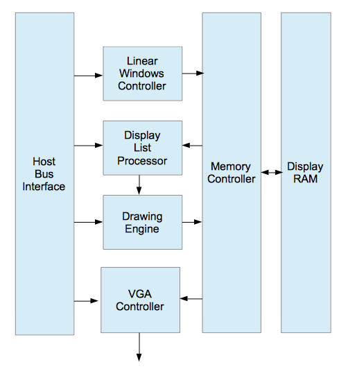
Here’s a quick overview of these components:
- Host Bus Interface Implements PCI bus protocol Allows the host CPU to write directly to display RAM or to registers that control internal card functions.
- Linear Windows Controller Performs color conversion and address translation/decoding for host transactions that read and write display RAM
- Display List Processor Reads lists of commands from display RAM and executes them to offload the CPU
- Drawing Engine Performs accelerated drawing operations, including 2D operations like lines and blits, and 3D triangle fills.
- VGA Controller Drive VGA timing and color signals, reading framebuffer data from display RAM.
- Memory Controller Drives control signals for internal display memory and arbitrates between functional blocks that access memory.
- Display RAM This stores a few things:
- Frame buffer: The VGA controller continually DMAs video data out of this to the screen and the rendering engine copies data into it.
- Source textures: The CPU must copy these into display RAM for the GPU to use it
- Display list: list of command parameters, discussed below.
This is a big project with over 5 million lines of code. But it’s organized fairly logically into subdirectories by function. The Verilog code is in the hdl/ directory. Here is an overview of the directories, which I’ve grouped together by area:
| Drawing Engine | de/ | 2D drawing engine and command processor |
| de3d/ | 3D drawing engine | |
| dlp/ | Display list processor | |
| lucy_tc/ | Texture cache | |
| math/ | Floating point math modules used by other blocks. | |
| Glue | include/ | Global defines |
| sim_lib/ | Simulator stubs (block memory, etc) | |
| top/ | Top level module for FPGA | |
| graph_core/ | Top level module for ASIC | |
| pll_intf/ | Phase locked loop clock generators | |
| hbi/ | Host bus interface | |
| generic/ | A generic FIFO that is used in other modules | |
| ram_based/ | Utility modules like async FIFOs. | |
| Memory Controller | mc_graph/ | Memory controller for on-board graphics RAM. |
| mc_cache/ | Some utility modules supporting the memory controller | |
| VGA Controller | clk_gen/ | Generates various clocks used by VGA |
| clk_switch/ | Generates CRT clock from pixel clock | |
| crt_sp/ | VGA display control registers | |
| vga/ | VGA output logic | |
| bios_internal/ | VGA BIOS ROM | |
| ramdac_sp/ | Various display functions, palette, cursor control | |
| FPGA Blocks | altera_clk_synth/ | |
| altera_ddr3/ | ||
| altera_ddr3_128/ | ||
| altera_ddr3_128_sim/ | ||
| altera_fifos/ | ||
| altera_plls/ | ||
| altera_project/ | ||
| altera_rams/ |
There is also an extra directory called de_temp that contains copies of many modules that are in de. It looks like it was perhaps a working directory or merge cruft. I sent an email to Frank Bruno, the author to ask about it. It had been a few years, so he didn’t remember the exact details, but also though it was probably just a working directory. I’ve ignored it here.
For now, I’m going to ignore the video card components and focus on the drawing engine. Also, I will focus on the 3D rendering operations and ignore 2D-only acceleration functions on GPLGPU like bit blits and lines. This functionality is in the de, de3d, lucy_tc, math, and mc_graph directories, a more manageable ~30k lines of code.
As I did with the VideoCore, I tried to trace the path of a triangle from the host interface to the screen and attached my notes here. Usual caveats apply: I’ve probably gotten details wrong or misunderstood some things. Corrections and clarifications are welcome.
Software Interface
After the CPU has performed vertex transformations and lighting, it initiates rendering by writing parameters for a triangle to control registers that are mapped into host memory. Section 2.3.6 of the documentation defines the memory map. Here are some of the registers:
| Register Address | Register Name | Description |
|---|---|---|
| 0x0050 | CMD_OPC | CMD Opcode Field |
| ... | ... | ... |
| 0x0178 | CP0 | Command Parameter 0 |
| 0x017c | CP1 | Command Parameter 1 |
| 0x0180 | CP2 | Command Parameter 2 |
| 0x0184 | CP3 | Command Parameter 3 |
| 0x0188 | CP4 | Command Parameter 4 |
| ... | ... | ... |
| 0x01D8 | CP4 | Command Parameter 24 |
| 0x01DC | 3D_TRIG | Trigger Register for 3D |
The meaning of the command parameter registers depends on the command opcode field. To draw a triangle, we will use the opcode TRIAN_3D (0x09), defined in section 5.8.15. Section 6.7 defines the parameters for the TRIAN_3D command:
| Register | Parameter | Format | Description |
|---|---|---|---|
| CP0 | PPTR | X-Y | Pattern Pointer |
| CP1 | V0_X | Float | Vertex 0 X |
| CP2 | V0_Y | Float | Vertex 0 Y |
| CP3 | V0_Z | Float | Vertex 0 Z |
| CP4 | V0_W | Float | Vertex 0 W |
| CP5 | V0_C | Int | Vertex 0 Color {A, R, G, B} |
| CP6 | V0_S | Int | Vertex 0 Specular |
| CP7 | V0_U | Float | Vertex 0 U |
| CP8 | V0_V | Float | Vertex 0 V |
| CP9 | V1_X | Float | Vertex 1 X |
| CP10 | V1_Y | Float | Vertex 1 Y |
| CP11 | V1_Z | Float | Vertex 1 Z |
| CP12 | V1_W | Float | Vertex 1 W |
| CP13 | V1_C | Int | Vertex 1 Color {A, R, G, B} |
| CP14 | V1_S | Int | Vertex 1 Specular |
| CP15 | V1_U | Float | Vertex 1 U |
| CP16 | V1_V | Float | Vertex 1 V |
| CP17 | V2_X | Float | Vertex 2 X |
| CP18 | V2_Y | Float | Vertex 2 Y |
| CP19 | V2_Z | Float | Vertex 2 Z |
| CP20 | V2_W | Float | Vertex 2 W |
| CP21 | V2_C | Int | Vertex 2 Color {A, R, G, B} |
| CP22 | V2_S | Int | Vertex 2 Specular |
| CP23 | V2_U | Float | Vertex 2 U |
| CP24 | V2_V | Float | Vertex 2 V |
Once we have programmed the values, writing the 3D_TRIG register from the previous table will start the rendering operation. Then the CPU must wait for the triangle to finish rendering before programming the next one.
Per the response from the author in the comments section, there are actually two sets of staging registers that allow the next command to be loaded while the previous one is being processed. The CPU still can only load one triangle at a time and must wait until a triangle finishes to load the next one.
If you have a lot of triangles, the CPU could spend a significant amount of time updating registers, which is the reason for the display list controller. It’s operation is pretty simple: the CPU writes lists of register values into display memory, and the display list controller jams the next ones in from the display list after it processes each command. Since the semantics of the commands are the same with the display list controller (and the rest of the drawing engine operates the same with either method of programming commands), I won’t talk about it any more.
Hardware Implementation
Let’s start by tracing what happens when the host writes to the GPU control registers. We’ll start at hdl/de3d/de3d_top.v. The inputs that deal with the host bus have the hb_ prefix:
       input [31:0]  hb_din,    // Data In
       input [8:2]   hb_adr_r,  // Host address
       input         hb_wstrb,  // Write Strobe (enable)
When we write each register, hb_wstrb (write strobe) goes high, indicating the data on the hb_adr/hb_din signals–which correspond to address and data–are valid. For example, here it writes command parameter 0 (vertex 0 X for a triangle command):
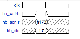
The de3d_reg (hdl/de3d/de3d_reg.v) module latches the value for all the 3D register parameters. A large chunk of this file consists of nested if/else statements that latch each register. For example, here is the code that latches the X coordinate of vertex 1:
        if (hb_adr==CP9) begin // V1X
            if (!hb_ben[0]) vertex1_u`VXB0 <= xy_in[7:0];
            if (!hb_ben[1]) vertex1_u`VXB1 <= xy_in[15:8];
            if (!hb_ben[2]) vertex1_u`VXB2 <= xy_in[23:16];
            if (!hb_ben[3]) vertex1_u`VXB3 <= xy_in[31:24];
        end
Writing the TRG3D register has the side effect of starting triangle rasterization. The code is in hdl/de/der_reg_1.v:
      /***************************************************************************/
      /*  LATCH THE COMMAND TRIGGER    */
      /***************************************************************************/

      // Hit XY1 or CP1 and not in 3D line or Triangle
      always @* cmd_trig_comb = (!hb_csn && hb_wstrb
            && (dlp_adr == {XY1_XY0, 1'b1}) && !hb_ben[3]) ||
            (!hb_csn && hb_wstrb && (dlp_adr == {TRG3D_CP24, 1'b1})
            && !hb_ben[3] && en_3d);
The cmd_trig_comb is an output of this module that kicks off a number of state machines that start filling the triangle.
Here’s a block diagram of the 3D pipeline:
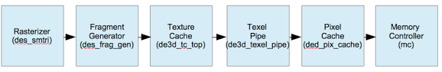
Every pipeline stage up to the pixel cache processes up to one pixel per cycle. This is different than VideoCore (and many other modern GPUs), which works on 2x2 quads.
Rasterizer
The rasterizer determines which screen pixels a triangle covers.
As we saw above, the CPU writes triangle coordinates to the GPU as three x/y raster positions. But the rasterizer uses edge equations. It is the job of the des_grad module (hdl/de3d/des_grad.v) to compute these values (gradients). The des_reg module latched those the vertex positions when the CPU wrote them as described above. All of these values are routed in parallel (448 bits per vertex) into the des_grad module:
     // Vertex Zero, One, and Two.
     input [447:0] vertex0,
     input [447:0] vertex1,
     input [447:0] vertex2,
When the CPU initiates triangle rendering after writing the vertex parameters, des_grad begins computing the rasterization coefficients. It has a floating point ALU module (hdl/math/flt_alu.v) that can perform a few operations in parallel. The des_grad state machine drives the ALU block to compute the coefficients for the rasterizer. It takes 42 cycles total to set up one triangle. It writes each coefficient as it computes it back to des_reg, which collects these and outputs them in parallel as a 256 bit wide signal called ‘spac_bus’. This connects into the scan converter module, called des_smtri, short for State Machine Triangle (hdl/de3d/des_smtri.v). As its name implies, this module implements a state machine that sweeps across the triangle, outputting up to one fragment position per cycle:
            output reg              t3_pixreq,
     output reg signed      [15:0]  cpx,  // Current position X.
     output reg signed      [15:0]  cpy,  // Current position Y.
When it has computed a pixel position, it asserts the t3_pixreq signal.
Fragment Generator
The fragment generator (hdl/de3d/des_frag_gen.v) performs the following operations for each pixel sent to it by the rasterizer:
- Interpolate parameters: U/V texture coordinates or ARGB color parameters, depending if texture or flat shading is enabled.
- Determine level of detail (which mip map to use) for texture fetches
- Perform 2D clipping to output rectangle.
This module outputs the raster position on screen and a bunch of computed parameters:
       output [15:0]  x_cur_o,      // Position of pixel
       output [15:0]  y_cur_o,
       output [31:0]  z_cur_fx,     // Z value for pixel
       output [19:0]  current_u,    // Texture coordinate
       output [19:0]  current_v,
       output [31:0]  current_argb, // Color value (for non-textured triangle)
       output [23:0]  current_spec, // Specular highlight
       output [7:0]   current_fog,  // Fog value
       output [3:0]   lod_num,      // Level of detail (mip map number)
The current_u and current_v (which are texture coordinates) feed into to the texture cache. The remaining parameters connect to a FIFO which feeds them to the texel pipe.
Texture Cache
The texture cache (hdl/lucy_tc/de3d_tc_top.v) receives U and V texture coordinates from the fragment generator. The push_uv signal goes high when a texel coordinate is available from the previous stage.
       input  push_uv,  // Push UV.
       input [10:0] current_u_g1,  // Upper left texel (U)
       input [10:0] current_v_g1,  // Upper left texel (V)
If the texel are in the cache, it will assert the ‘tc_ready’ signal and outputs four adjacent texel color values in parallel.
     output [31:0] ul_tex,         // Upper left texel
     output [31:0] ll_tex,         // Lower left texel
     output [31:0] ur_tex,         // Upper right texel
     output [31:0] lr_tex,         // Lower right texel
If the texture cache does not have the texel in question, it will stall while it fetches the data from the memory controller. It will assert tc_ready when the data is available. The texture cache supports a number of source color formats and performs color conversion as necessary.
Texel Pipe
If texturing is not enabled, the texel pipe (hdl/de3d/de3d_texel_pipe.v) ignores the output of the texture cache. But let’s assume it is for now. When the texture cache asserts the tc_ready signal, the texel pipe will retrieve both the texture color from the texture cache and pop the other fragment parameters out of the FIFO that the fragment generator put them in.
The texel pipe performs the following operations:
- Blend/filter the four raw texels from the texture cache (bilinear filtering).
- Apply fog
- Alpha reject test
- Convert pixel color to destination format (for example, RGB565)
- Dithering. The output device only supports 16 bits per pixel, so this was required to compensate for that. Modern output devices support more color depth, so this an obsoleted component.
When the texel pipe has a valid computed position, it asserts ‘pc_valid’ and sends the formatted pixel and position information to the pixel cache:
       output reg [31:0]   formatted_pixel, // Color to Pixel Cache
       output reg [7:0]    current_alpha,   // Alpha to Pixel Cache
       output reg [15:0]   x_out,           // X Position
       output reg [15:0]   y_out,           // Y Position
       output reg          pc_valid,        // Load Pixel Signal to Pixel Cache
The Z values from the fragment generator bypass the texel pipe via a FIFO and are delivered to the pixel cache in the same cycle as the other data.
Pixel Cache
The pixel cache is contained in the ded_top module (hdl/de/ded_top.v). It instantiates submodules prefixed ‘ded_’, which stands for “Drawing Engine Datapath.”
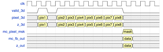
Up until this point in the pipeline, everything has worked on a pixel at a time. But the memory controller works in 128 bit chunks (this GPU was advertised as “128 bit” graphics card, this is presumably what they were referring to). At 16 bits per pixel, that is eight pixels. The pixel cache collects the pixel data and sends a full burst in parallel to the memory controller:
       input   valid_3d,
       input [31:0]   pixel_3d,              // Color data for pixel
       input [31:0]   z_3d,                  // Z data for pixel

       output [BYTES-1:0]  mc_pixel_msk,     // pixel mask data output
       output [(BYTES<<3)-1:0] mc_fb_out,    // Color out
       output [(BYTES<<2)-1:0] mc_fb_a,      // Alpha out
       output [(BYTES*8)-1:0] z_out
We can see this in action below. The valid_3d signal indicates when a pixel is ready from the texel pipe. Once all of the pixels are collected, the pixel cache will push all 128 bits of the data (both Z and frame buffer data) out, along with a mask that indicates which pixels were covered. Near the edge of a triangle, it’s possible not all eight pixels overlap the triangle, in which case the 8 bit mask will indicate this.
Memory Controller
The memory controller module (hdl/mc_graph/mc.v) combines a number of functions. It arbitrates access to internal memory from internal sources like the display list processor and the VGA controller. But for our discussion, the important part is performing final operations on the pixels and writing them back to the frame buffer. This includes alpha blending and Z-Buffer checking. These operations require reading existing data from the frame buffer:
- To get the existing Z value to compare to the newly generated one
- To get the existing color value to be alpha blended with the new one
- To write the old value of pixels that are not covered by the triangle because they are past the triangle edge or fail to the depth test (since the memory controller can write only a full 128 bit burst to memory) The memory controller reads the existing pixels and Z-buffer data from graphics memory, storing them in the mc_mff module (hdl/mc_graph/mc_mff.v). This presumably happens at the same time the earlier stages of the pipeline are generating pixels. The physical interface to memory is 64 bits wide, so it takes two cycles to read color data and two more to read Z data.
When a batch of eight rendered pixels arrives from the graphics pipeline (via pixel cache), and the destination data is available from graphs memory, the mc_dat (hdl/mc_graph/mc_dat.v) module performs blending and z-buffer operations on all eight pixels in parallel. The module hdl/mc_graph/mc_dat16.v performs the alpha blending and raster operations for a pixel. You can see here that it instantiates an array of these, one for each pixel:
      mc_dat16 mc_dat[(BYTES/2)-1:0]
        (
         .mclock                (mclock),
mc_dat handles Z-testing. A case statement selects the comparison based on the Z-operation. The loop instantiates logic for each pixel that sets new_z_mask according to the check
      always @(posedge mclock)
        if (z_pipe[1])
          casex({pix_i[0], z_op_i})
            ...
            {2'bx1, LESS}:
            for (loop0 = 0; loop0 < BYTES/2; loop0 = loop0 + 1)
              if (de_zdata_i[loop0*16+:16] < z_store_i[loop0*16+:16])
                new_z_mask[loop0*2+:2] <= 2'b00;
              else
                new_z_mask[loop0*2+:2] <= 2'b11;
After the memory controller processes the pixels, it writes the pixel colors back to the framebuffer in display memory.