Keeping Score
I recently embarked on a complete redesign of the microarchitecture for the GPGPU I’ve been working on, with a major goal being to increase the clock frequency. The previous version had a maximum frequency of around 30 Mhz when synthesized for my Cyclone IV FPGA board, constrained by some long combinatorial logic paths. One way to increase clock speed is to break stages apart, making the pipeline deeper. This, however, is not without tradeoffs. it increases the latency of each operation (in terms of clock cycles), and introduces new pipeline hazards. Combined together, these can decrease the performance of the CPU. I’ve attempted to mitigate this by utilizing a technique used by a number of modern GPUs (which was in-turn borrowed from early out-of-order microprocessors, although in this context it is used for in-order issue).
A read after write hazard (RAW) occurs when an instruction is dependent on the result of the previous instruction that has not completed. For example, imagine the following sequence of instructions:
reg1 = reg2 + reg3
reg4 = reg1 + reg5
The second instruction depends on reg1. If the first instruction takes several pipeline stages to complete, then these cannot be issued back-to-back. In the previous microarchitecture, simple instructions such as integer addition or bitwise logical OR had only one cycle of latency. A forwarding network bypassed results from later stages to reduce the latency (clock cycles) of the pipeline. Complex operations such as floating point instructions, were tagged as ‘long latency’ instructions. When the CPU issued these, it would suspend the thread until the instruction completed–regardless of whether subsequent instructions had dependencies or not. The problem was that this forwarding network was a long combinatorial path with a lot of delay and was the critical path for clock speed.
In the new design, all instructions are now ‘long latency’. A simple integer operation like addition or bitwise logical and has a latency of 3 cycles (versus 1 previously). A floating point add or multiply has a latency of 7 cycles (versus 4 previously).

This design hides latency by using multiple hardware threads. When a thread is suspended on a long latency result, other threads can be scheduled. The previous design used four threads per CPU core. It would be possible to increase the number of threads to cover the increased latency. However, threads aren’t free. Each thread consumes around 17kbits of SRAM for the register file and the register file is triple ported (two read ports and one write port).
Often, it is not necessary to suspend a thread because back-to-back instructions don’t have a dependency. Ideally, we would only suspend a thread when necessary. If that could be done without adding many gates, the result would be a performance boost without the cost of increasing the number of threads.
This problem seems a bit tricky because of the need to look at the previous six issued instructions. However, a much simper mechanism called a dynamic scoreboard solves this neatly. It’s pretty simple:
- Each thread maintains a busy bitmap with one bit per register. This tracks which registers have results pending.
- Each time an instruction is issued, the busy bit corresponding to the destination register for that instruction is set.
- Each time a result is written back to the register file, the busy bit corresponding to the destination register is cleared.
- A dependency bitmap is computed with one bit for each source register for the next instruction to be issued for that thread.
- Each cycle, the thread scheduler perform a logical AND of the busy and dependency bitmap. If the result is non-zero, the instruction cannot be issued from that thread in that cycle.
It’s not enough for something to seem like it will perform well. We’d like some empirical results. I ran a few permutations of this design in Verilog simulation to verify that my assumptions were correct. This design is using a placeholder for the L2 cache and system memory interface, so latency to main memory is not accurately modeled, but I don’t think that should have significant effect on the results. I used a similar benchmark configuration to a previous post. The test program renders a Phong shaded teapot with 2300 triangles into a VGA framebuffer and measures total cycles. The rendering engine, written in C++, is around 3000 lines of source code and compiles to 16k of code and 59k of read only data (most of which is geometry data for the model).
I ran two tests: one with the scoreboard active and one with it disabled by setting the dependency bitmap to all ones. Here are the results:
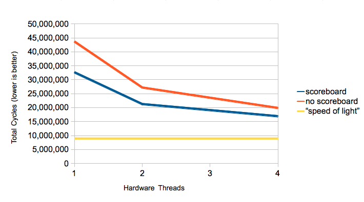
The “speed of light” (a term a hardware designer I knew liked to use) represents the minimum number of instructions that must execute to finish the program, assuming an instruction is issued every cycle with no squashes (this is the sort of number many vendors put in their marketing materials :) The fundamental goal of this design is to decrease the number of dead cycles by keeping the execution unit is busy as possible. Note that the performance difference between the scoreboard the non-scoreboard implementation gets smaller as the number of hardware threads increases. Hardware threading and the scoreboarding are different methods of hiding instruction latency, with the latter being less expensive, but bounded in how much it can reduce latency.
The numbers seem to suggest the scoreboard was a good design choice.