VideoCore QPU Pipeline
As a followup to the last post, I’ve taken a closer look at the Quad Processor Unit that executes shaders on the VideoCore GPU. Although it superficially looks like a CPU, there are some important fundamental differences, and the reasons for them are interesting.
Here’s a simplified version of the QPU’s compute pipeline from figure 2 (p. 17) of the VideoCore Architecture Guide.
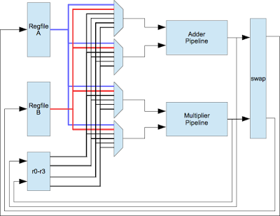
The first notable thing about this diagram is that the main register file is split into two banks: regfile A and regfile B. Instructions encode which bank each operand comes from. There are constraints around how these registers are used: An instruction can only fetch one operand from each bank. For example, the following is fine, because it fetches register 7 from bank A and register 4 from bank B:
fmul ra1, ra7, rb4
But the next one is illegal. It tries to fetch both register 7 and 13 from bank A.
fmul ra1, ra7, ra13
This constraint exists because each bank only has one read port. This differs from most CPUs (and Nyuzi), which have one register file with at least two read ports and can use any combination of register operands without restriction.
To understand this design decision, it’s first useful to talk about how ports are synthesized–specifically on ASICs.
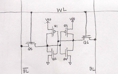
The following is a simplified schematic of a single bit inside an SRAM. This is called a 6T cell because it has six transistors. Q1, Q2, Q3, and Q4 form a latch: a pair of cross coupled inverters. A bunch of cells like this are arranged in a 2D grid. A word line signal (WL) connects all cells on the same row, and two bit line signals (BL), which are inverses of each other, connect to all cells on the same column. When a specific word line is activated–only one ever is–all latches on that row are connected to the bit lines via Q5 & Q6. The bit lines are read or written at the bottom or top edge of the array (when writing, the column drivers overpower the latch transistors).
This port can read or write one value at a time. To perform an independent access in parallel, another port is needed. This requires an extra word line per row, a new pair of bit lines per column, and two additional transistors (Q7 & Q8) per cell to connect them:
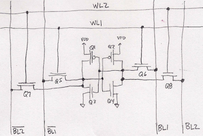
This makes everything physically larger, and the connecting wires longer, which uses more power.
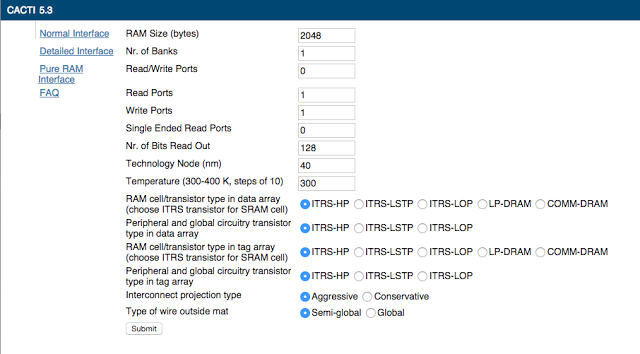
I can quantify this using a tool called CACTI (Cache Access and Cycle TIme), which builds an electrical model of the wires and transistors in the SRAM array and estimates its area, power usage, and latency. Full source code to the tool is available here, but an online version is also available:
http://quid.hpl.hp.com:9081/cacti/sram.y
First, I’ll compute the parameters for the QPU as it is described in the documentation. Each entry in the register file has 16 SIMD lanes (times four bytes per entry is 64 bytes per register). There are 64 registers, which is 4096 bytes per QPU. I divide this by two in the computation because there are two register banks (I’ll multiply the resulting area by two again).
The documentation repeatedly refers to the register memories as ‘single ported’, but I believe they are referring only to the read ports and these memories must have both a read port and a write port for the result:
- Otherwise instruction issue would need to stall for every retired instruction that writes back to the register files, which would have pretty crummy performance.
- This would require extra logic to detect collisions. This would be odd, since they don’t detect other, simpler types of hazards (for example, on p. 37, the mention that “An instruction must not read from a location in physical regfile A or B that was written to by the previous instruction” because there is no bypassing)
The QPUs each have four execution pipelines that they issue the same instruction to four times to process all sixteen vector lanes, so the register file needs to read four vector lanes at a time (128 bits).
Given these parameters, I can use the CACTI to characterize the register files (Note that the “Nr. of Banks” parameter for CACTI has a different meaning than “banks” as I’ve been referring to here, so I keep it 1).
The result:
Total read dynamic energy per read port(nJ): 0.00454679252507
Total standby leakage power per bank (W): 0.00109152252016
Total area (mm^2): 0.0342587754656
I multiply the area and power by two because there are two banks:
Read port power = (0.00454679252507 nJ * 250 MHz + 0.00109152252016 W) * 2
banks = 2.27 mW
Area = 0.193458538913 * 2 = 0.0685175509312 mm^2
Let’s now compute values for a CPU-like version with two read ports and one write port. This would allow using all registers as operands without constraints. Since this isn’t longer banked, I don’t halve the memory size.
Total read dynamic energy per read port(nJ): 0.00791710847258
Total standby leakage power per bank (W): 0.0028442195272
Total area (mm^2): 0.0932270438867
Read power = 0.00791710847258 nJ * 2 ports * 250 MHz + 0.0028442195272 W = 3.96 mW
The area is 2.7x larger and it uses 1.7x as much power, which seems to justify the VideoCore designers decision to use single ported memory (especially as there are 4 QPUs per slice and at least 3 slices).
Each register bank has 32 general purpose registers, for 64 total. That’s more than most CPUs, and there is a good reason for it: they can’t be spilled. The QPUs don’t have load and store instructions, and consequently no stack, so there’s nowhere to put them.
In the QPU diagram, there are four more general purpose registers in the lower left (r0-r3), which are referred to as accumulators in the documentation. These can be used without restriction as any operand or destination. They are useful as temporaries to work around these register constraints.
These temporaries also enable another optimization. There are separate, 3-stage pipelines for addition and multiplication. In most CPUs, each instruction can encode a single operation. However, if VideoCore did that, half of the stages in either pipeline would always be idle. That is something no GPU designer can bear. Instead, the VideoCore QPU uses a 64-bit wide instruction which can encode both operations to execute simultaneously. This is an example of a design principle seen throughout this chip: keep every functional unit as busy as possible. This diagram from figure 3 (p. 27) shows how instructions are encoded:
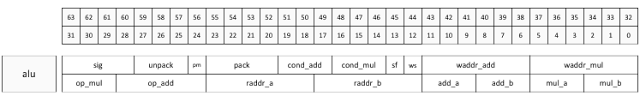
The add_a, add_b, mul_a, and mul_b fields control the four multiplexers in the center of the pipeline diagram above. These can select one of the accumulator registers, or a result from one of the banked register files. The raddr_a and raddr_b fields form addresses into the two register files for read, and the waddr_add/waddr_mul control the write port address. This introduces another constraint: the add and multiply instructions cannot write their results to the same bank.
For comparison, if the architecture supported two operation instructions without any constraints, it would require a register file with four read ports and two write ports:
Total read dynamic energy per read port(nJ): 0.012013930148
Total standby leakage power per bank (W): 0.00469288164114
Total area (mm^2): 0.292972180628
Read port power = 0.012013930148 nJ * 4 ports * 250 MHz + 0.00469288164114 W = 12.01 mW
This is 8 times larger than the actual design and uses 5 times as much power.
This instruction encoding impacts code size. In the case where it can pair add and multiply operations in the same instruction, this is no difference in size than having two 32-bit instructions. However, it may not be possible to pair them if and add and multiply don’t occur successively in the program, or if there is a bank conflict. Instructions that aren’t ALU operations, like load_immediate or branches cannot be paired with other ones and consume an entire 64 bit instruction. So, the code is most likely going to be larger, but, since shaders are fairly simple and there aren’t a lot of them, this seems like an appropriate tradeoff (unfortunately, since the shader compiler seems to be hidden inside a binary blob, it’s tough to tell how much overhead this introduces).
In summary, there are some key differences between the QPUs in VideoCore and a general purpose architecture like Nyuzi:
- VideoCore does not have load/store instructions.
- It needs a larger register file to accommodate all temporaries.
- This eliminates the need for a data cache, making the QPUs smaller
- The QPUs are less flexible (for example, they don’t support recursion) and require specialized external hardware to access in-memory data structures.
- VideoCore uses banked register files to save power and area, but this makes the compiler more complex and requires extra instructions to transfer results to/from accumulators.
- VideoCore uses 64-bit wide instructions that can encode multiple operations, at the cost of larger code.
While the use of load store instructions, and the larger instructions are tradeoffs that would be inappropriate for Nyuzi’s use cases, it’s interesting to explore if there would be an advantage to using banked registers on Nyuzi.
The default configuration for Nyuzi has two read ports and one write port. There are four threads with 32 vector registers, which are 512 bits wide for each. The read and write ports are 512 bits wide. For simplicity, I’ll ignore the scalar register file, which is much smaller than the vector one. The RAM size is 64 bytes per reg * 32 regs * 4 threads = 8192 bytes
Total read dynamic energy per read port(nJ): 0.0426987452745
Total standby leakage power per bank (W): 0.00431499044499
Total area (mm^2): 0.680605555836
At 250Mhz, this results in:
0.0426987452745 nJ * 2 ports * 250Mhz + 0.00431499044499 W = 21.35 mW
This is for a core with four threads. The previous numbers for VideoCore were computed per QPU, of which there are four in a slice (a VideoCore slice and roughly equivalent to a Nyuzi core, both having sixteen execution units and four effective threads of execution). If we multiply the previous numbers, we end up with ~ 9.08 mW of power for a VideoCore slice, about half that of Nyuzi.
Now let’s examine an alternative version of Nyuzi with two registers banks:
Total read dynamic energy per read port(nJ): 0.0302475000381
Total standby leakage power per bank (W): 0.00201081979371
Total area (mm^2): 0.298628831583
The power is now 0.0302475000381 nJ * 2 banks * 250 Mhz + 0.00201081979371 W = 15.12 mW
The area is 0.597257663166 mm^2
The non-banked version of Nyuzi is 1.1x times larger and uses 1.7x times as much power as the banked version would.