The Mystery of the Missing Pixels
One goal when I started my GPGPU project was to be able to display 3D graphics with my FPGA board on a VGA monitor. This required me to add an SDRAM controller, since there is not enough block SRAM on the FPGA to contain an entire VGA framebuffer. I managed to execute code running out of SDRAM on the processor, and display static images on the monitor. But, to my dismay, when I tried to render animations in real time, the monitor displayed garbage. I imagined all kinds of gnarly data corruption bugs that could exist in the SDRAM controller. Stepping through millions of memory transactions to find the problem was enough to make me want to go back to writing software.
The VGA controller and CPU share memory through an arbiter.
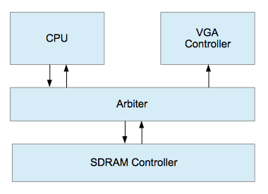
The VGA controller connects to a digital to analog converter (DAC) that drives the analog red, blue, and green color signals to the monitor. It needs to fetch 640 * 480 pixels * 4 bytes per pixel * 60 frames per second to refresh the screen, or 70 MB/second. The VGA dot clock is 25 Mhz, so it must drive a new pixel to the display exactly every 40 nanoseconds while in the middle of a scan line (it doesn’t need to drive them during horizontal and vertical blanking periods).
My first working hypothesis was that the SDRAM controller was not delivering data fast enough to the VGA controller, because, frankly, that was an easier problem to debug.
A Digression on Memory Bandwidth
Before talking about the problem and how I solved it, it’s useful to talk in more detail about the memory subsystem.
Below is a simple program that runs on Nyuzi and attempts to saturate the memory interface. I’m going to start by profiling reads only for simplicity. I’ll demonstrate that these results are applicable to writes and copies. This test performs vector wide reads to improve throughput to the L1 cache. The vector width is the same as a cache line, so each read instruction will cause a cache miss. Because the pointer is volatile, the compiler shouldn’t optimize away the reads.
#define LOOP_UNROLL 16
volatile veci16_t *src = (veci16_t*) region1Base;
veci16_t result;
int transferCount = kTransferSize / (64 * LOOP_UNROLL);
do
{
    result = src[0];
    result = src[1];
    ...
    result = src[15];
    src += LOOP_UNROLL;
}
while (--transferCount);
Words like shouldn’t always make me a bit nervous, so, just to be sure, I dumped the assembly output. There are 16 unrolled load instructions in a row (a total of 1024 bytes), followed by a few instructions to update the pointer and loop:
.LBB0_1:
    load_v v0, (s0)
    load_v v0, 64(s0)
    load_v v0, 128(s0)
    ...
    load_v v0, 960(s0)
    add_i s1, s1, -1
    add_i s0, s0, 1024
    btrue s1, .LBB0_1
I ran this in Verilog simulation with a simulated SDRAM chip that mimics the one on my FPGA board. The SDRAM is single data rate (one transfer per cycle) with a 32 bit wide interface, so the maximum speed is four bytes per cycle. Based on the execution of the time of this test, I computed an average of 1.3 bytes per cycle, utilizing about 32% of the bus capacity.
This processor uses the AMBA AXI protocol to communicate with the memory controller. I won’t spend much time diving into that protocol here–there are really only two signals we need to look at for the purposes of our analysis. The m_arvalid (read address valid) signal indicates the host is requesting a new read transfer, and the s_rvalid (read data valid) indicates when the memory controller is responding with data. Here is a waveform of this test running in Verilog simulation:
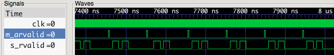
There are a number of things going on here, but it’s useful to look first at the m_arvalid signal. The distance between each processor request is 48 cycles. During that time, it performs 16 transfers (times 32 bits per transfer, the width of the SDRAM interface = 64 bytes, which is the size of a cache line). This matches the results I measured above.
This test was only using one hardware thread. As we’ve seen in previous posts, hardware threads can improve utilization and hide memory latency. I modified the test to use four threads, fetching interleaved addresses:
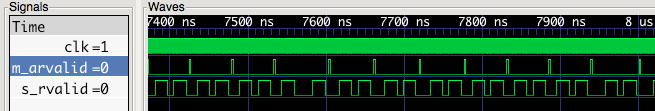
This test transfers an average of 2.3 bytes per cycle, utilizing about 57% of the memory bandwidth. It fills a cache miss every 27 cycles. This is much better, trimming off 21 cycles per cache miss.
In the single threaded case, the thread is blocked during those 21 cycles. Among other things, this delay includes the restarted L2 fill moving through the L2 cache pipeline, the time for the next instruction to move through the instruction pipeline, another pass through the L2 cache pipeline for the subsequent cache miss, as well as delays for various intermediate queues.
This processor delay is completely removed by using four threads. How can I be sure? There is a FIFO in the L2 cache that contains pending read misses. I added a print of the number of entries in this FIFO every clock cycle:
    always_ff @(posedge clk, posedge reset)
    begin : update_gen

        ...

        $write("%d ", sync_fifo_pending_load.count);
As you can see, this FIFO is never empty. The execution pipeline is no longer a bottleneck and all of the remaining delay is inside the L2 cache.
There’s something satisfying about using printfs to debug hardware. It just seems kinda wrong.
There are still 11 remaining cycles that are wasted. What happens to those? Let’s zoom in a little more closely. The trace below includes the SDRAM control signals: CS (chip select), RAS (row access strobe), CAS (column access strobe), and WE (write enable). These signal names originated with non- synchronous DRAM, but in SDRAM don’t retain much of their original meaning. They encode an arbitrary four bit operation, which is documented here.
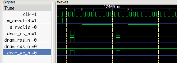
The first gap is four cycles between point A & B.
The first cycle is the the time to accept the request and advance the SDRAM controller state machine. In this test configuration, the processor is connected directly to the SDRAM controller, so this only takes 1 cycle. In many real world system-on-chips, CPU requests usually travel through an interconnect, and one or more clock domain crossings. A latency of around 20 cycles is not uncommon. The AXI request and response channels are independent to allow a host to send the next request before the data transfer for the first one is completed. This would mitigate this delay, but Nyuzi doesn’t support this yet.
In the second cycle, the control signals are asserted to SDRAM to perform a read. After the command is issued, it takes two cycles for the first byte of burst data to come out. This interval is referred to as ‘CAS latency’. This is assuming a relatively slow clock. For modern DDR3 SDRAM, for example, this can be anywhere from 8-16 cycles.)
The last cycle of this is delay in the FIFO between the SDRAM output and AXI.
The second gap is between C & D. SDRAM transfers data in fixed size bursts of 8 transfers. The processor has requested a burst of 16 transfers (each is four bytes, total of 64 bytes). So, in the middle of the transfer, the SDRAM controller needs to send another read command to set up the next SDRAM burst. The timing of this is similar to the gap between A & B, except the first cycle is related to the state machine transition in this case.
The remaining gap of two cycles is between E & F. My L2 AXI fill state machine has a state to indicate read completion, then goes back to the idle state before checking for the next transaction. Restructuring the state machine could shave off these two cycles.
Before the controller can read SDRAM, it must ‘activate’ the row is is going to read from. This is involves connecting one of the rows of capacitors to the array of sense amplifiers. My SDRAM controller lazily leaves rows open after activating them, so most of the time it skips this step, as it did in the trace above. Most modern SDRAM controllers do this, and, just to throw a little more confusing terminology in the mix, the scenario where a row is not already open is referred to as a “DRAM page miss.”
Below is an example where the controller needs to activate a row. There are three commands in a row starting at marker A (A command is active when dram_cs_n is low):
- A precharge command to close the existing row
- An activate command to open the new row
- A read command to read the data, as in the previous examples
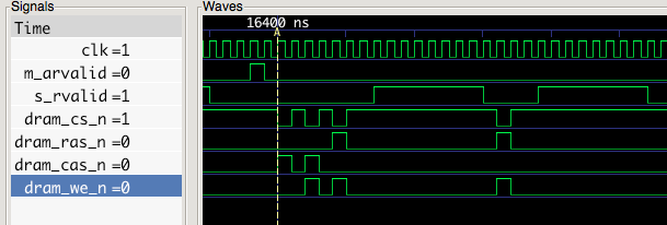
One notable thing about this trace is that the commands aren’t issued back to back. The datasheet for this part indicates that between the precharge and activate commands, there must be a delay of 21 nanoseconds (this is denoted tRP or Row Precharge Time). The clock here is 50 MHz, which is a period of 20 ns–just a hair short–so I use a delay of two cycles. Likewise, between the activate command and the first read command, a 21 ns delay is required (this is tRCD or RAS to CAS delay). Because the clock rate is low for this configuration, it’s only a few cycles, but the number of clocks would increase as the clock rate did.
For this test, it’s only necessary to open a row when the copy crosses a 32k boundary (this size is based on the physical layout for this specific part). But this is a well behaved access pattern, which has a DRAM page hit rate of 65%. A random access pattern would need to activate rows more often, which would reduce throughput.
Here are the test results for write and copy tests, which are structured similarly to the read test and are using four threads:
copy: 0.99220066 bytes/cycle
read: 2.18565583 bytes/cycle
write: 2.18943238 bytes/cycle
The write test is similar to the read test because it involves similar bus transactions. The copy test reports about half the speed of either because it needs to do two memory transactions per byte. Multiplying the read number by the 50 MHz clock rate gives a best case transfer rate of 115 MB/second. This is about 57% of the “speed of light” of the SDRAM if it were able transfer every cycle with no delays. This is a pretty typical utilization for real world systems in my experience.
The Problem with Fairness
Given the numbers computed above, I can compute a rough memory bandwidth budget for the problematic use case. If SDRAM has a peak transfer rate of 115 MB/second and the VGA controller needs 70 MB/second, this leaves 45 MB/second for the CPU. But if the CPU and VGA are accessing different rows in the same bank, they will end up causing more DRAM page misses which will reduce this number.
I made the arbiter prioritize the VGA controller for reads, knowing bandwidth was tight and that it couldn’t tolerate delays (when the VGA is in the middle of a scan line, it must deliver a new pixel to the VGA DAC exactly every 2 cycles or 40 nanoseconds). As it turned out, there were a few problems:
- The AXI protocol treats read and write channels independently, as did my arbiter. The SDRAM controller can only handle one at a time, so it pingponged between writes and reads.
- The the burst length for the VGA controller was half that of the CPU, so, when it did ping pong, the CPU would get 2/3 of the bandwidth, and the VGA would only get 1/3.
To make sure things were properly stacked unfairly in favor of the VGA, I prioritized reads in the SDRAM controller and increased the VGA burst size to twice of that of the CPU. This change addressed what I confirmed was a VGA underrun issue, but introduced a horrible, subtle race co ndition that would cause some programs to hang after running for around 30 seconds on FPGA (1.5 billion cycles). This took me far longer to debug than the original problem.